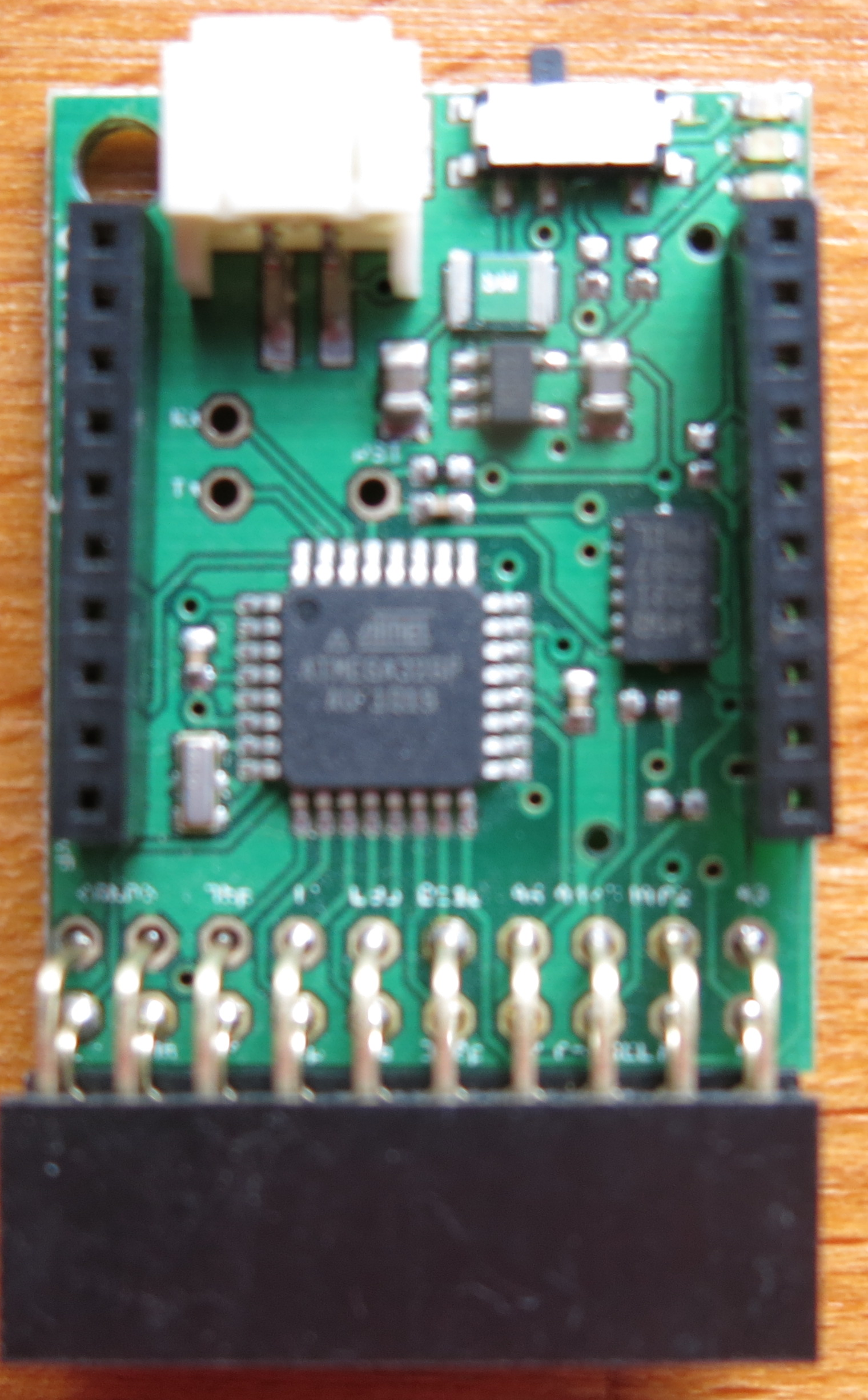
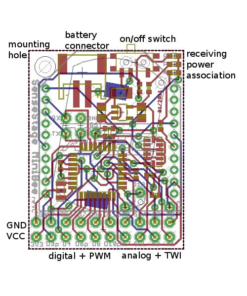
MiniBee Revision B
The MiniBee revision B was the second version of the MiniBee, the beta version. It was manufactured during the research-creation project Sense/Stage at Concordia University and McGill University in 2010. It was only distributed to those who were somehow involved in the project at that time, and some may still be around at Concordia University in Chris Salter’s lab or in the IDMIL lab at McGill University. The overview of the board is given here for historical reference.


Overview of the board:
- 6 analog inputs: A0, A1, A2, A3, A6, A7
- 9 digital inputs or outputs: D3 to D11
- PWM (“analog”) output, at pins D3, D5, D6, D9, D10, D11
- I2C communication: SDA (A4), SCL (A5)
- Serial I/O: RX, TX (to XBee)
- Power input (between 3.3V and 5V), through battery connector and coin cell battery
- Regulated power output: 3.3V, GND
- green pcb
Pin out
The pin outs on the header are from left to right:
GND - GND - D5 - D7 - D9 - D11 - A6 - SDA - A2 - A0
3v3 -  D3 - D4 - D6 - D8 - D10 - A7 - SCL - A3 - A1
LEDs
Technical documents
Board layout and schematic are available here: design files for Eagle on github
Changes to previous version
Revision B of the board has several improvements over revision A:
- Faster resonator (12 MHz), allowing for higher baudrates
- A fuse to protect the circuit
- Smaller footprint
- One-way battery connector
- Coin cell holder footprint on the back for coin cell battery
- On/off switch
- Flow control for communication between XBee and ATmega chip
- ATmega328P instead of ATmega168, so more program and data memory
- Reset pin broken out (mostly useful for getting the bootloader onto the board)
Programming firmware and bootloader
For programming the firmware, use the board definition: Sense/Stage MiniBee revB/D/F (3.3V, 12MHz) w/ Atmega328p
| page created on: | last changed on: |
|---|---|
| 6 February 2017 | 4 September 2019 |
